DesignWorks


Visit my other pages:


DesignWorks
DesignWorks is available for both Macintosh OS X and Windows. Features that make the package valuable to me include:
Unlimited number of attributes per design, device or signal, and can be categorized as primary or secondary.
Large, up to 32,000 character values for attributes, large enough to hold a Spice model, long html links, or whatever!
Flexible scripting language for error checking, net lists, generating web based orders, building libraries,
generating FPGA & CPLD user constraint files, connector pinout tables, merging text files with device attributes, and such.
The scripting language can generate and launch AppleScripts.
Attribute Browser for device and signal attributes. It looks like a spread sheet and behaves similar to one.
Optional digital simulator and compatible with MacSpice.
Automatic page and grid location with page connectors updated live.
Hierarchical and flat schematics.
Flexible printing options.
Design kits separate different tasks, like Spice, block diagrams, and circuit design.
Auto-create symbol tool for fast symbol generation.
You can see the whole list of attributes I use here. I am also using DesignWorks to design my Raspberry Pi Zero HAT board, see it here.


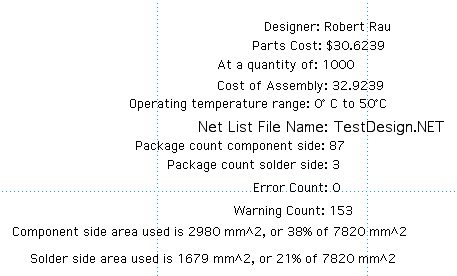
On the right is my extended title block text. Most of these design attributes are computed in scripts. The last two lines are the board area use summary.
The next two lines are the text you place in your schematic to see the results.
Component side area used is &AreaCompUsedmm2 mm^2, or &AreaCompUsedPct% of &AreaCompmm2 mm^2
Solder side area used is &AreaSoldUsedmm2 mm^2, or &AreaSoldUsedPct% of &AreaSoldmm2 mm^2
You can download my Area script, RPArea111.rfm.zip here. You can download my attribute setup script, AttrSetup153.rfm.zip here, but you may need to edit it first so it doesn’t mess up any of your attributes.
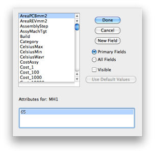
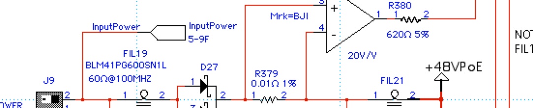
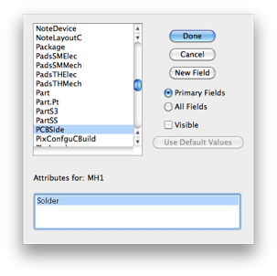
One of the scripts I use in circuit design is my PCB area calculator. I use this to know the amount of board area that is used during the schematic capture process. This uses design attributes that describe the area available on the component and solder side of the PCB. It also uses two device attributes; one for the area used on the side of the PCB the device is placed, and one for the area used on the other side of the board. Most SMT parts only use one side of the board unless they have an exposed pad that needs heat sink vias. There is also a device attribute that indicates which side of the board the part is mounted. See the device attributes left and center below. This script does not generate a report file, it only updates the design attributes for used board area for each side, and the percent used board area for each side.
PCB ‘Area Used’ Script
This is my Osmond net list report for flat designs. This makes the format I use in my Device Placer application if you need components place in circles. You can download it from here:
A header on the top of the net list includes the circuit name, assembly, revision, and designer (from design attributes), and the date. The nets that start with KS, for Keep Short, are listed first.
Attributes it uses:
Device
&package
Design
&DevUsedLast
&UnitsUnused
&Assembly
&Revision
&Designer
Osmond PCB Layout Net List Script
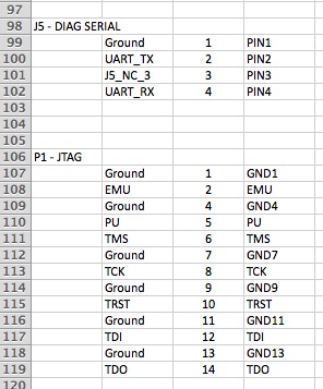
Connector Pinout Script
This is my script for making an Excel spread sheet of pinouts of all my connectors. Any device in the schematic with a Name.Prefix attribute set to J, P, TB, or SP (Jacks, Plugs, Terminal Blocks, or Solder Pads) will be included.
Attributes it uses:
Device
$PINNAME
&Name.Prefix
$PINNUM
$DEVNAME
Signals
$SIGNAME
The output format of each connector is Signal Name, Pin Number, Pin Name. In the examples at the right, J5 is a generic connector, so the Pin Names are generic. P1 is a connector for a specific purpose, so its Pin Names are specific to that connector.
Capacitor Count Check Script Fragment
This is just a piece of my design check script. Unlike many of my checks in that script, this just makes sure an attribute is filled in or of a proper format. This script fragment will check to see that there is at least one capacitor (&Name.Prefix is C) for every device (&Name.Prefix is U) pin on power supply nets. Power supply nets must start with “Plus” or “Minus.” After I had tried and failed to make a script to do this, the staff at Capilano, now DesignWorks Solutions, figured it out for me.
Attributes it uses:
Device
$PINNAME
&Name.Prefix
Pin
&ExtraPins
Signals
$SIGNAME
&ccount (temporary)
&CountWarning (temporary)
&ucount (temporary)
&ulist (temporary)
In recent releases of OS X the ~/Library folder is invisible. To get to the design kits with the libraries, templates and reports, you need to go to
~/Library/Application Support/DesignWorks/Design Kits
This link shows you how to make the ~/Library folder visible:
http://www.ifixit.com/Guide/Making+Visible+the+Users+Library+Directory+in+OS+X+Lion/9618
Now you can easily get to the documentation at ~/Library/Application Support/DesignWorks/Documentation
The User Guide will tell you how to set up your Design Kits so you have access to your libraries, Templates, and scripts/reports.
To customize you own schematic template, you will want to use these two menus:
Drawing -> Custom Sheet Info...
Drawing -> Design Preferences...
if you click the "Use Page Setup" radio button in Custom Sheet Info then you will also need to set up page size and scale in File -> Page Setup.
I prefer to print on tabloid size paper (11x17). I also like smaller gates and text than the default. So I set page setup in my template to 11x17 and 58% reduction.
I also use a fairly involved attribute system. I have written a script (report with no output) to setup my template attributes. You can download my attribute Attribute Setup.rfm.zip and modify it as you wish.
Some Things You Need To Know


DesignWorks

Other DesignWorks Resources On My Site
I have several DesignWorks libraries including some Infineon, NXP & Freescale ARM processors, and all SMT resistor standard values from 0201 to 2512 for both 1% and 5%. Other libraries include Analog Devices, Texas Instruments and many passives. You can find them here.
I have written a few tools to make library creation easier. One tool helps with Xilinx FPGAs, another tool can create files to make libraries of any group of devices where the part number and the part value have a sequence and a simple relationship. Most manufacturers resistors, capacitors, inductors, and zener diodes fall into this requirement. I have other tools to add location information to DesignWorks net lists for Osmond to place components in circles. These applications can be found here.